

Short abstract:
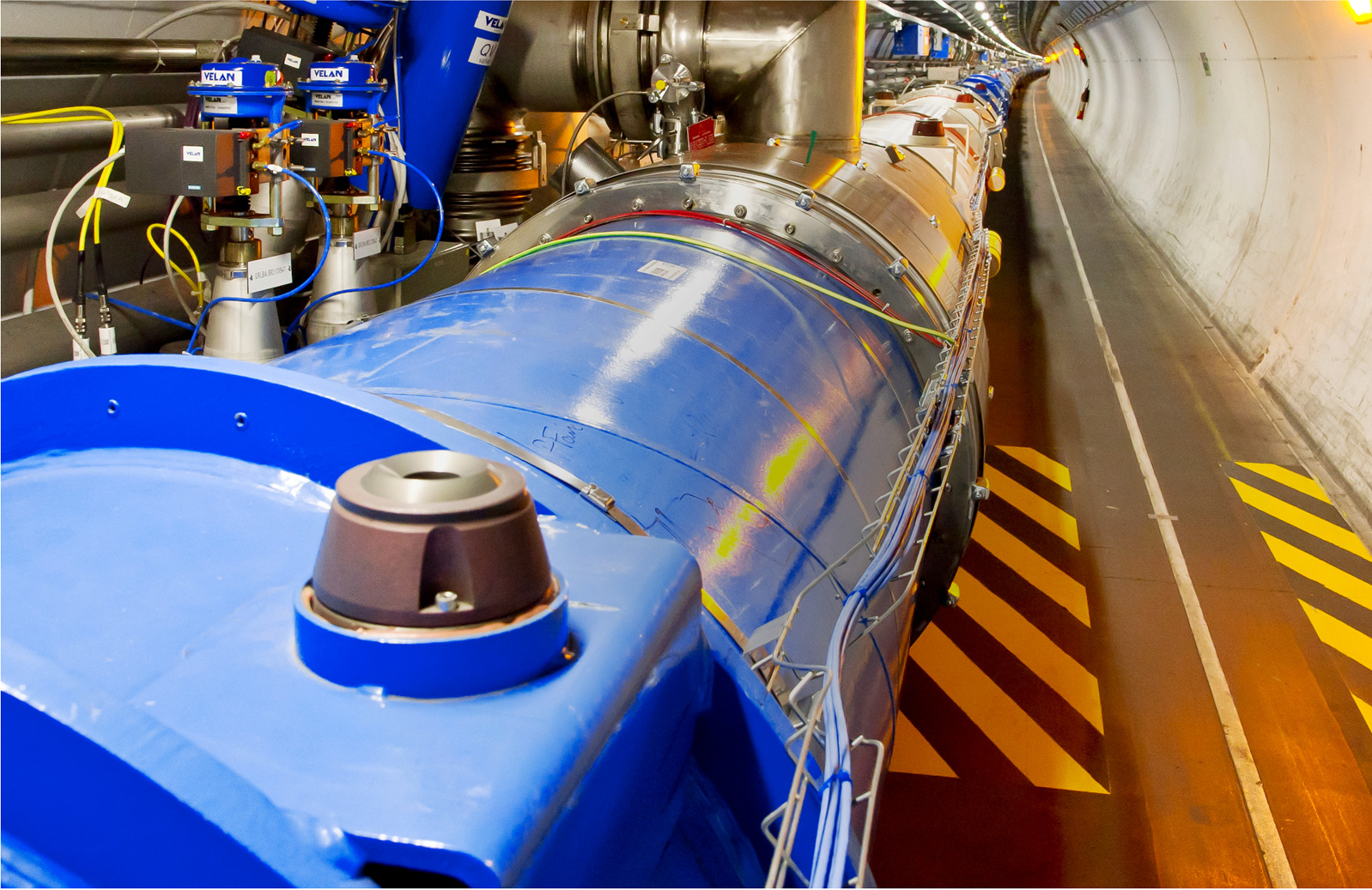
The goal of this PhD project will be to lay the circuit foundations for radiation tolerant, time-based, analogue signal processing to support the needs of future nuclear systems like thermonuclear fusion reactors (e.g. ITER) and high-energy physics experiments (e.g. HL-LHC), as well as challenging space missions (e.g. JUICE), where the electronic front-ends will be exposed to extreme levels of radiation up to 1000 times higher than current commercial rad-hard components can handle. Scaled CMOS technologies are often impacted by a reduced dynamic range of the signals, and therefore benefit from processing signals in the time domain. Since time accuracy is severely impacted by radiation, which increases 1/f noise and mismatch in oscillators and delay lines, innovative radiation tolerant low-jitter circuits are needed to achieve ps-accuracy. This project sets the innovative goal to develop a radiation tolerant sub-ps time-to-digital converter and a 16-bit time-based sensor readout in nanometer CMOS technologies with record radiation tolerance of 10 MGy and 3·1016 neutrons/cm2 (1 MeV) to make this possible. The project will collaborate with ESR8 for modelling aspects, profit from the predictive tools developed by ESR9 and ESR10 and from the study of synergetic effects by ESR3.
Long abstract:
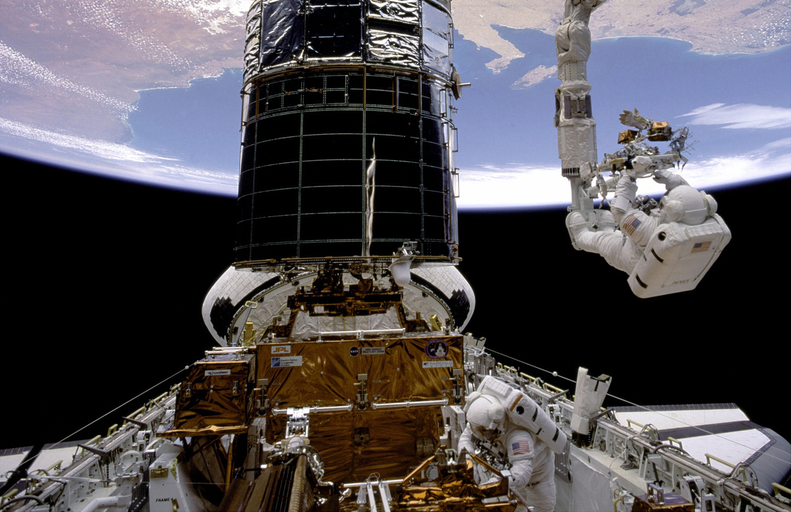
This project will lay the circuit foundations for radiation tolerant, time-based, analog signal processing to support the needs of future nuclear systems like thermonuclear fusion reactors (e.g. ITER) and high-energy physics experiments (e.g. HL-LHC), where the electronic front-ends will be exposed to extreme levels of radiation up to 1000 times higher than current commercial radhard components can handle. Proposed developments are also in-line with the needs for increased radiation hardness in the space community.
Instrumentation systems for current nuclear applications are based on signal conditioning circuits, which process sensor signals in the voltage domain. For this purpose only a limited number of radiation hardened components like amplifiers and Analog-to-Digital Converters are available on the market and the radiation tolerance is limited to only a few kGy. Progressively scaled CMOS technologies have shown potential for high radiation tolerance. Unfortunately their lower operating voltage reduces the dynamic range of the signals. Therefore, it has become more interesting to process signals in the time domain where the analog information is stored in the zero transitions of a signal. Their accurate processing now requires radiation tolerant low-jitter circuits with sub-ps-accuracy which are impossible to achieve with state-of-the-art knowledge.
Unfortunately with technology scaling, the sensitivity to single-event effects (SEEs), caused by individual particle strikes, increases dramatically owing to the small node capacitances. It has also been shown that ionizing radiation increases 1/f noise and worsens mismatch problems. These effects have a huge impact on the accuracy of time-domain circuits. Indeed, the TDC relies on accurate delay cells, processing the start and stop signals. In this project innovations will be proposed to allow automatic and continuous recalibration of individual delay cells to achieve sub-ps performance in the presence of ionizing radiation. Innovative architectural, circuit and layout techniques will be unraveled to allow radiation tolerant time-accurate signal processing with sub-ps accuracy in nanometer CMOS technologies. Circuits will be designed to function up to a targeted dose of 10 MGy a neutron fluence up to 3E16 1 MeV neu/cm2 and an SEL immunity up to 150 MeV.cm2/mg. This project will target sub-ps time-to-digital conversion and a 16-bit time-based sensor readout with the required extreme radiation tolerance.
This project will benefit from the SEE predictive tools that will be developed in WP2.9 at Univ. Montpellier II, and from the study of TID and SEE synergistic effects in WP1.3 that will be hosted at CERN. Finally since the proposed approach is linked to asynchronous digital circuits, a good degree of interaction with WP2.6 on modeling and test methods of coupled radiation and ageing constraints on complex digital integrated circuits, also hosted at Univ. Montpellier II
Deliverable & Milestones Lists:
- Report on technology selection and architecture definition.
- Report on the design and measurement of a radiation tolerant Time-to-Digital Converter.
- Report on the design and measurement of a radiation tolerant time based sensor readout circuit.
- Completed development of a radiation tolerant time based sensor readout circuit.
Beneficiary:
KU Leuven
Supervisor:
Prof. Paul Leroux (KU Leuven)
Co-supervisor:
Prof. Vincent Pouget (Univeristy of Montpellier)
Planned secondments:
[total: 8 months]: MAG (Dr Y. Cao): [2m] For support in design and manufacturing of component SCK•CEN (Dr W. de Cock): [2m] For neutron and gamma irradiation testing, CERN (Dr S. Danzeca): [2m] For mixed field radiation testing at CHARM, UM (Dr V. Pouget): [2m] For SEE laser testing and hardening techniques
Position has been appointed to Arijit Karmakar. Click here for Profile.