

Short abstract:
Current CMOS image sensors have a limited radiation tolerance owing to radiation induced degradation of the pixel dark current and noise levels which massively degrades the dynamic range of pixel intensity. The challenging innovation in this PhD project is the development of new APS topologies and readout architectures for CMOS image sensors with a radiation tolerance of 1 MGy, SEL immunity up to 150 MeV.cm2/mg and integrated single-event corrections. This will enable the design of a radiation tolerant CMOS imager prototypes with a target resolution of 1280x720 and a frame rate of 60 fps. Other research works have shown the possibility to extend the electronic device lifetime by applying heating cycles. This thermal annealing approach will also be investigated in this PhD in order to reach high dose levels. This type of imagers will be indispensable for remote handling applications and increasing safety and security in todays’ and future nuclear reactors, for monitoring applications in high energy physics, and for space-applications, particularly nano-Startrackers development for LEO (Low-Earth Orbit) satellite applications.
Long abstract:
This PhD project targets the design and assessment of a radiation tolerant CMOS imager in mainstream CMOS technologies. A CMOS imager consists of a matrix of Active Pixel Sensors (APS), containing photodiodes whose charges are collected with a sensitive amplifier and an integration capacitor per pixel. The pixels are read out sequentially by column ADCs to determine each pixel’s brightness. Current CMOS image sensors have a limited radiation tolerance owing to radiation induced degradation (increase) in the pixel dark current and noise levels which massively degrades the dynamic range of pixel intensity. The most radiation tolerant imager available on the market today is the STAR1000 chip sold by On Semiconductor. The chip features a pixel matrix of 1024x1024 and is able to withstand a dose of 100 kGy. However it was implemented in a 0.5 m CMOS technology and is limited to a full image frame rate of 11 fps. Moreover there is a drastic increase of the average dark signal with the accumulated dose of radiation of about 25 e-/s/Gy (shown valid up to 0.5 kGy [http://www.onsemi.com/pub/Collateral/NOIS1SM1000A-D.PDF]). For a nominal prerad dark signal of 200 e-/s, this means that after 0.4 kGy the dynamic range of pixel intensity is already degraded by about 34 dB or almost 6 bit.
Current research in radiation tolerant CMOS imagers focuses on the use of thin gate oxide rings around the photodiode perimeter to minimize the total ionizing dose induced degradation at the Silicon interface. The challenging innovation in this PhD project is the development of new APS topologies and readout architectures for CMOS image sensors with a radiation tolerance of 1 MGy, Single-Event Latch-up immunity up to 150 MeV.cm2/mg and integrated single-event corrections. The goal is to achieve this with current commercially available CMOS processes by using radiation-hardening by design techniques including off-set compensation, low-frequency noise rejection, calibration and auto-zeroing to compensate for the radiation induced non-uniform increase in dark current and dark noise levels. Moreover, based on the understanding of the degradation mechanisms, we propose to investigate, in this PhD, the effect of a thermal annealing approach used to extend devices lifetimes [1], [2]. Annealing will induce a detrapping of radiation-induced-charges, and a recovery will occur: the electronic device is regenerated. This will pave the way for the design of a radiation tolerant CMOS imager prototype with a target resolution of 1280x720 and a frame rate of 60 fps.
A modeling study mainly based on use of the E.CO.R.C.E software [3] will be also performed in this PhD project. E.CO.R.C.E., a new TCAD modeling tool developed in the Montpellier 2 University, allows simulating in 2D electronic devices at the physical level. The main feature of this tool, is that the dose effect in oxide can be modeled (trapping, transport and de-trapping). Moreover, E.CO.R.C.E. also takes into account the heat equation. This new feature coupled with transport equations and coverage of trapping phenomena, will allow the study of annealing effects in the oxide of devices during and after irradiations, which is useful for investigating the regenerative method.
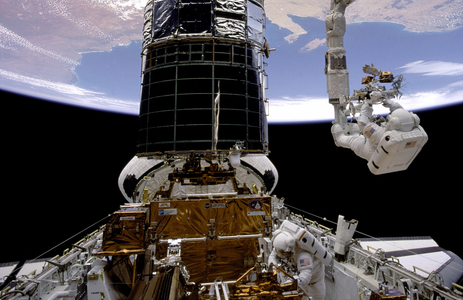
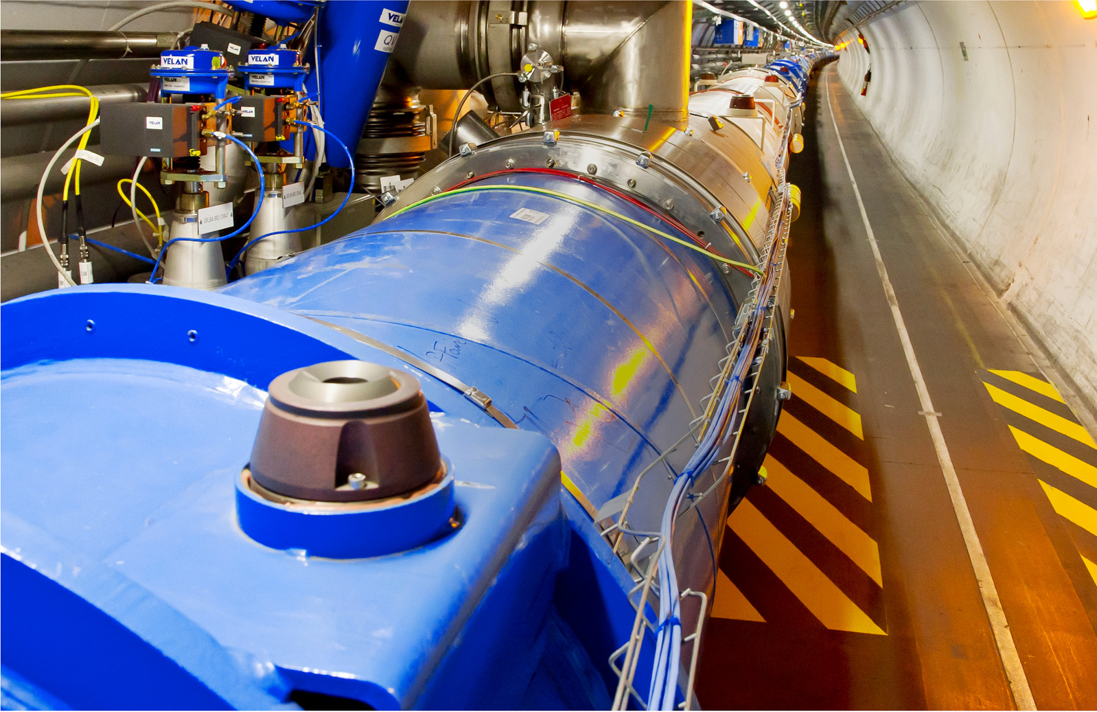
This type of imagers will be indispensable for remote handling applications and increasing safety and security in todays’ and future nuclear reactors and for monitoring applications in high energy physics, but also for instance in nuclear waste monitoring. This type of imagers can also be a solution for the challenging deep space missions, such as the jovian missions, where the radiation environment will be much more restrictive than for previous space missions and for other space-applications, such as the development of nano-Startrackers for LEO satellite constellations.
This PhD project is linked to several other PhD projects in the network. The project will build on the insights obtained in the PhD project of WP1.3, hosted by CERN, where the aim is to understand the synergistic effects in mixed field radiation environments. It will also build on the predictive tools for assessing radiation tolerance, to be developed at University Monpellier II in WP2.9. The project may also offer an interesting component for a stacked (3D) system as targeted in WP3.12 on the development and radiation assessment of a System-In-Package (SiP).
Deliverable & Milestones Lists:
- Report on technology selection and architectural study.
- Report on the design, measurement and modeling of elementary CIS components.
- Report on the design, manufacturing and testing of APS, integrated Column ADC and periphery circuits.
- Report on the design and measurement of a radiation tolerant CMOS imager.
- Completed development of a radiation tolerant CMOS imager.
Beneficiary:
KU Leuven
Supervisor:
Prof. Paul Leroux, Prof. F. Tavernier (KU Leuven)
Co-supervisor:
Prof. Jérôme Boch (Univeristy of Montpellier)
Planned secondments:
[total: 10 months]: MAG (Dr Y. Cao): [1m] For component design and implementation; UiO (Assoc. Prof. K. Roed): [1m] for FPGA and automated imager readout; SCK•CEN (Dr W. de Cock), CERN (Dr S. Danzeca) and RUG (Dr E. van der Graaf): [3m] For neutron, gamma and proton irradiation testing and dedicated tests in representative environments (CHARM); UM (Dr J. Boch): [3m] For the thermal annealing approach and for the understanding of the physical mechanisms (TCAD simulation); CNES (J. Mekki): [2m] For specifications and constraints related to space environment and characterizations with the CNES test benches.
Position has been appointed to Rico Maestro. Click here for Profile.
[1] S. DHOMBRES, A. MICHEZ, J. BOCH, F. SAIGNÉ, J.-R. VAILLE, S. BEAUVIVRE, D. KRAEHENBUEHL, P. C. ADELL, E. LORFEVRE, R. ECOFFET, "Study of a Thermal Annealing Approach for Very High Total Dose Environments", IEEE Transactions on Nuclear Science, vol.61, no.6, pp.2923,2929, Dec. 2014.
[2] F. ROIG, J. BOCH, F. SAIGNE, L. DUSSEAU, J.R. VAILLE, A. TOUBOUL, P.C. ADELL, E. LORFEVRE, R. ECOFFET, "A Thermal Annealing Approach to Extend Metal Oxide Semiconductor Devices Lifetime Exposed to Very High Dose Levels", RADECS2012, Biarritz, 2012.
[3] A. Michez, J. Boch, S. Dhombres, F. Saigné, A. D. Touboul, J.-R. Vaillé, Laurent Dusseau, E. Lorfèvre, R. Ecoffet, "Modeling dose effects in electronics devices: Dose and temperature dependence of power MOSFET." Microelectronics Reliability 53(9-11): 1306-1310 (2013).